Projects id Electronic Devices that Underpin the Era of 5G History of challenges and forecasting of the future
From the First Year of 5G to “Beyond 5G” Current developments of GaN HEMTs that continue to evolve
GaN HEMTs are manufactured by combining state-of-the-art equipment with outstanding human skills (Yamanashi Plant, Sumitomo Electric Device Innovations, Inc.).


Challenges to increase the diameter of wafers and downsize packages
Many chips can be cut out from a large-diameter wafer. One of the important themes in the initial phase of mass production was to reduce costs by increasing the wafer diameter. Mass production of GaN HEMTs started using two-inch wafers. Production using three-inch wafers was achieved in 2007, and production using four-inch wafers was achieved in 2011. Wafer processing involves about 100 processes, and changing the wafer diameter means the entire rearrangement of apparatuses and materials. To optimize the production process, problems were solved one by one. Hitoshi Haematsu, who currently works in the Device Production Engineering Dept. of SEDI, is one of the members who worked on the challenge.
“Wafer processing consists of a front surface process to form electrodes and a back surface process to thin wafers and cut them into chips. SiC, which is used for the substrate, is an extremely hard material. Wafer thinning technology for SiC was unavailable anywhere in the world. We tried to grind wafers forcibly using a robust grindstone, but the yield was poor and the processing speed was low. We contacted a manufacturer of back surface grinders and developed an innovative grinding technology. The processing speed increased dozens of times compared to the conventional method. Defects caused by grinding were almost eliminated,” recalls Haematsu.
Efforts were also made to downsize packages to accommodate the GaN HEMT chips. Norihiro Yoshimura, who currently works in the Electron Device Development Dept., #1 of SEDI, was one of the members in charge.
“We had to meet the cost requirements of customers. This was an important factor to beat Si-LDMOS transistors. Downsizing of packages translated directly into cost reduction. We worked on downsizing by changing the circuit system in the package and design methodology. The size has been reduced to one fourth compared to that in 2006, achieving total cost reduction,” says Yoshimura.
The low power consumption of GaN HEMTs also helped reduce the cost spent by base stations. GaN HEMTs were gradually accepted in the market. The communication carriers that used GaN HEMTs praised such characteristics as high output, high-speed transmission and low power consumption, and the recognition by the market followed. GaN HEMTs started to be known as “monster devices.” GaN HEMTs were rapidly accepted by the market when the communication protocol shifted from 3G to 4G and the required frequency bandwidth expanded with the advent of the era of high-speed and large-capacity communication. It is noteworthy that GaN HEMTs contributed to the downsizing of base stations. The power consumption of GaN HEMTs was low, which achieved low heat generation and eliminated the need for air cooling fans and other components. This helped reduce the size and weight of base stations, making the installation work easy and expanding the installable areas. The number of small base stations, which are called remote radio heads, increased sharply. GaN HEMTs were also used for terrestrial digital broadcasting transmitters and the Skytree broadcasting station. In 2013, the sales of GaN HEMTs skyrocketed in line with the growing demand outside Japan. In 2014, SEDI won the Minister of Education, Culture, Sports, Science and Technology Prize at the Technology Management and Innovation Awards for various accomplishments in the telecommunications field.

Expanding global market share of GaN HEMTs
The year 2020 is regarded as the first year of 5G. There has been an intense competition in the market between GaN HEMTs and Si-LDMOSs as transistors for base stations. SEDI has the top market share in GaN HEMTs for base stations, and in 2019 its sales were close to that of the top supplier of Si-LDMOSs. The sales of GaN HEMTs have been very strong, but the situation does not allow for an optimistic outlook. Global Si-LDMOS manufacturers have been preparing to knock SEDI off the table before GaN HEMTs becomes the mainstream. To ensure differentiation, it is necessary to improve GaN HEMTs. Isao Makabe, who works in the Electron Devices Dept. of the Transmission Devices Laboratory of Sumitomo Electric Industries, Ltd. is one of the members in charge. He is engaged in the development of thin film crystal growth technology, which is the core technology for GaN HEMTs.
“Die shrink has been further accelerating for high-frequency devices of 5G and beyond. It is important to develop crystals suitable for the structure. The current GaN HEMTs have a structure in which crystals of GaN and AlGaN are layered to generate electrons on the bonded interface. What is interesting about GaN is that the device behavior can be changed significantly by controlling the Al-Ga ratio and film thickness. My mission is to pursue novel GaN HEMT crystals that meet the characteristics, mass productivity and cost advantage,” says Makabe.
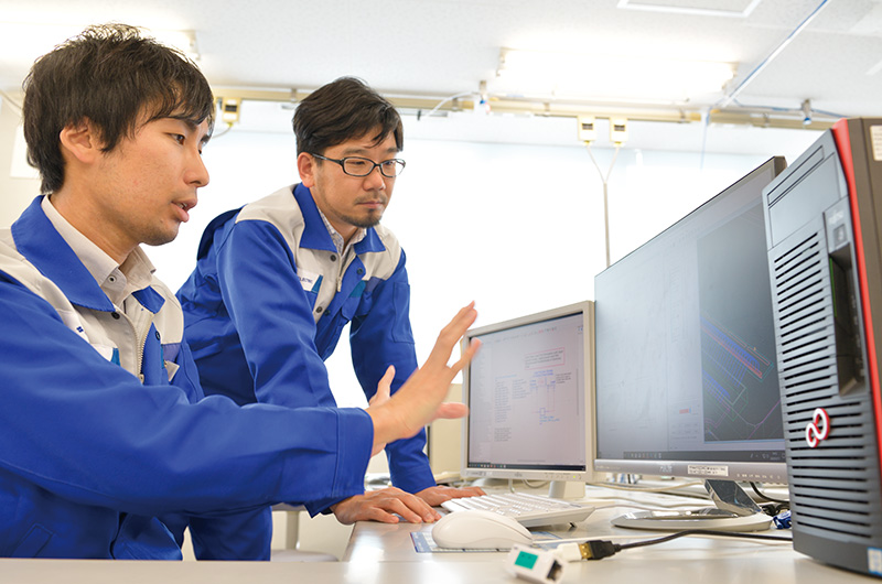
Ken Kikuchi from the 5G-Radio Dept. of Transmission Devices laboratory is in charge of the operation analysis and modeling of GaN HEMT chips.
“The device requirements vary depending on the customer and application. I am responsible for identifying potential risks and problems during actual operation of devices at base stations and giving feedback to the device development team. The development of evaluation and simulation techniques is an important research topic. The potential of GaN HEMTs is very high, and there is still much room for further development. We serve as an intermediary between technology development, including crystal growth, and product design to accelerate the device development,” says Kikuchi.
Along with these efforts, wafer processing technology has been developed, which is supervised by Inoue.
“Adaptation of GaN HEMTs to the high-frequency band requires further process shrink. For example, electrodes must be fabricated in the order of nanometers, which is thinner than the AlGaN and GaN layers. However, semiconductor processing requires high energy. Die shrink and the thinning of HEMTs cause damage to semiconductor due to the processing energy. We are developing processes to clear the hurdles. We envision communication technologies beyond 5G. The frequency band is millimeter-wave bands of 28 GHz or more. Expansion of the use of high-frequency bands means that the devices will become thinner. In this context, process development will become even more important,” says Inoue.
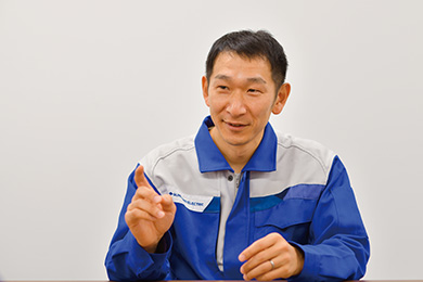
Right) Isao Makabe, Assistant General Manager , Electron Devices Dept., Transmission Devices Laboratory, Sumitomo Electric Industries, Ltd.