Home > Product Index > InP Sub > InP Sub p type
GaAs Substrates
InP Substrates
GaN Substrates
Epitaxial Wafers
[ Download PDF version formatted for print : 712KB ]
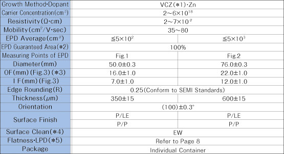
(*1) VCZ:Vapor Pressure Controlled Czochralski (*2) EPD Guaranteed Area:Percentage of points within spec. (*3) High Precision OF(±0.02°)is available for 2"φ. (*4) EW:Etched Wafer (*5) LPD:Light Point Defects
- Standard
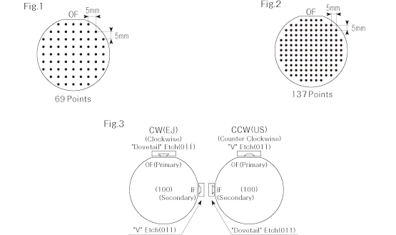
Resistivity・Mobility・Diameter・OF・IF・Thickness (min.~max.) EPD Map
- Option
Accuracy of Orientation・Flatness・Light Point Defects
Semi-Insulating
n type
p type
Other specifications